unrepairable A2251 820-01949-A board >>> SSD, T2 transplant

yozas

New member
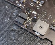
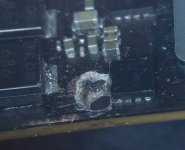
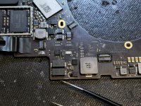
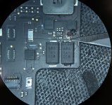
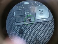
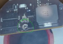
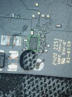
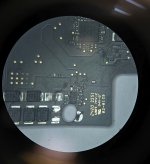
Greetings, I have a board 820-01949-A i5 16GB 512GB where the cap C7053 (sitting on PPVBAT_G3H_CHGR_REG rail) started burning and the damage got deeper into the layers of the PCB. It did not look too bad and I was quite optimistic, but as soon as I started digging into the charred PCB, I saw that it spread quite widely inside, the charring area has even reached under the corner of U7000 itself, so further drilling/cleaning would definitely mean destroying the U7000 ISL9240 pads and is pointless.

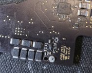
I need to do a data recovery, so I am preparing to buy another working motherboard for that purpose. I have checked the SSD power supply rails to estimate if there is a chance that the SSD chips survived, and have found no shorts, the lowest voltage drop reading is on the PP0V9_SSD0 rail, about 0.107V one way, 0.305V another way, but I guess it's normal for this rail?

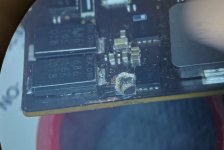
I have also checked for any clear signs of dead T2 chip (because I will have to transfer it along with SSD chips, correct?) and haven't found any. Also tested all the pads under U7000 ISL9240 against GND for shorts (because some are going to the T2 chip), and found no shorts.

The question is, what do I need to do to make the SSD chips work and their data be accessible after transferring them to another (working) motherboard?
I am sure that I have to transfer the SSD chips (lovely job 🥰) and the T2 chip, but is there anything else that would need to be done?
Like transfer the U4770 SPI chip that is connected to the T2 chip, or edit serial number in it? Probably swap the Touch ID sensor also, right?

Or would I have to transfer the CPU (because of some ME engine/CPU serial stuff that can possibly be bound to the T2?) also for it to work?

Oh, and should I care if the board that I'm going to buy is locked in some way or not?
Also, should I care if that board config differs from current one? What differences are allowed? CPU? RAM? SSD?
In case of SSD capacity difference I guess I would have to configure the BOARDID1,BOARDID2,BOARDID3,BOARDID4,BOARDID5 strap resistors, correct?
Or how does the board determine the SSD capacity? By checking the info that is inside the T2/T2 SPI (those I can transfer)?

My soldering and electronics skills are excellent, fixing motherboards for 20 years, but I don't know any of these "apple specific" nuances.

Thank you!
 

2informaticos

Administrator
Staff member
First of all, welcome to the forum!

If no chance to clean the short, you can try to swap NANDs together with T2.
Better to replace the SoC ROM too; make backup for both.

Check if both boards have the same SSD size.
Put the configuration straps as in original board.
If the new board can be detected into DFU, an Apple authorized workshop can recover the data in DFU mode.
If you need to get the board fully working (no access to Apple server), then don't do DFU restore; it will erase SSD.

Did you find any feedback about such swap on Internet?

One thing you can try, not sure if works however.
Remove F7000 and be sure no short on any other areas, apart of its pad 1.
Then apply 12V on pad 2 and check if board appears into DFU.
Check then if SSD voltages are present too; can try DFU revive, if not.
If you get SSD powered, data recovery can be done.
However, as T2 lost communication with U7000, this option may not be possible; just for try.
 

yozas

New member
Good day, and thank you, yeah there is no chance to clean the short, as further drilling that needs to be done would wipe off the U7000 ISL9240 soldering pads, it is already really close, and I am sure that a lot of internal layer traces got burned/damaged in the process already. It is impossible to tell. I will attach some photos just for some fun.

So I bought a locked board with a 256GB SSD, as the price was really good, now waiting for it to arrive. So I guess I will have to config the straps BOARDID1,BOARDID2,BOARDID3,BOARDID4,BOARDID5 just in case. Currently I don't even know if they will differ from the current board, and if these straps are related to the SSD size in any way. But I will check them just in case.

I haven't found any straps related to SSD size, but internet says that the SSD size info is programmed into the SSD chips themselves (and there are devices to flash them, including remaining lifetime/wear info).
And maximum supported (means it can be lower) SSD size limit is determined by the T2 chip internal RAM size (I have read that there are 1GB and 2GB versions).

Anyway, it does not matter, because I will transfer the original T2 chip so it should prevent any potential mismatch if there would be any, correct?
I need to transfer it anyway because of SSD crypto keys that exist inside of it.


And of course I have tried to at least remove the short from main power rail from all of its sides, but it seems that it is not possible, at least not without destroying the ISL9240 charger controller pads, because more PCB drilling is needed to clear the charring.
Going further would definitely mean that ISL9240 would lose the communication with T2, so in my eyes it's a dead end. Waiting for a 256GB board to arrive and then I will continue.


I have checked the schematics for other potential chips to be transferred besides SSD, T2, T2 flash, that could possibly be bound to the old system, and this is the list I have made. Let's start.

You wrote that I need to transfer the SoC ROM.
U4770 - T2 SoC SPI flash

But what about SEP EEPROM? Because it is also connected to the T2.
U4730 - T2 SEP EEPROM (SEP = secure enclave processor, I guess?)


The WIFI/BT system. It consists of the WIFI/BT chip and SPI flashes connected to it. I have read somewhere that people fixing apple stuff had to transfer the whole WIFI/BT chip, because some info is stored inside of it. Maybe it was on a model where the WIFI chip did not have external SPI chips, I'm not sure.
U3730 - WIFI/BT chip
U3750 - BT SPI flash
U3710 - WIFI SPI flash


I'm not sure what is this one, but the schematics page that it's on is named "Secure element". It is connected to the T2 chip.
U5000 - Secure element
Here is some information I found about this "Secure element":
The Secure Element is an industry-standard, certified chip running the Java Card platform, which is compliant with financial industry requirements for electronic payments.
The Secure Element (or SE) is the NFC/ApplePay chip.
Apple's Secure Element is a tamper-resistant hardware component that is designed to store cryptographic keys and perform secure operations. It is used to store sensitive information such as payment credentials and biometric data on Apple devices. The Secure Element is designed to be secure by using a combination of physical security measures, such as anti-tampering mechanisms and secure boot processes, as well as software security measures, such as encryption and access controls.


Keyboard controllers I2C EEPROM, not sure I need to transfer it, but theoretically it can be needed, right?
U6700 - I see that this I2C EEPROM is connected to the keyboard mux/expander chips (U6701, U6702)


The SPI flashes that are connected to USB-C and Thunderbolt controllers:
U3060 - Thunderbolt/USB-C controller SPI flash
UB260 - Thunderbolt/USB-C controller SPI flash


Also the Intel CPU/PCH U0500 may need transferring, because it has stuff programmed into its management engine, which theoretically may be included in the secure T2 etc. binding system. Well, at least in PC systems when you change the PCH or CPU/PCH combo, you have to do a "Clear ME" procedure, because the old ME config stored in the PCH is bound to the ME config stored in the BIOS/UEFI chip.
And because in this macbook we do not have a separate BIOS/UEFI chip (because the Intel UEFI boot firmware is stored in the T2 as I understand), it means that old T2 will "look for" the old CPU that has the PCH ME region config which corresponds to the ME region config stored in the T2, correct?

At least to me it looks like I will have to transfer the CPU/PCH also, in order to avoid ME region conflicts, as even if the original one manages to boot up, there can be stutter/slow boot/max fan problems until I perform a DFU restore.


What do you think? Thank you very much!
 

Attachments

  • 20240226_170008.jpg
    20240226_170008.jpg
    971 KB · Views: 3
  • 20240226_170212.jpg
    20240226_170212.jpg
    369.7 KB · Views: 3
  • 20240226_170217.jpg
    20240226_170217.jpg
    302.6 KB · Views: 3
  • 20240226_170308.jpg
    20240226_170308.jpg
    365.3 KB · Views: 3
  • 20240226_170536.jpg
    20240226_170536.jpg
    987.9 KB · Views: 4
  • 20240226_171148.jpg
    20240226_171148.jpg
    704.2 KB · Views: 4
  • 20240227_125509.jpg
    20240227_125509.jpg
    620.1 KB · Views: 4
  • 20240227_130643.jpg
    20240227_130643.jpg
    717.4 KB · Views: 3
  • 20240227_131900.jpg
    20240227_131900.jpg
    690.4 KB · Views: 3
Last edited:

yozas

New member
some more
 

Attachments

  • 20240227_131900.jpg
    20240227_131900.jpg
    690.4 KB · Views: 5
  • 20240227_131004.jpg
    20240227_131004.jpg
    479.3 KB · Views: 5
  • 20240226_165950.jpg
    20240226_165950.jpg
    547.4 KB · Views: 5

2informaticos

Administrator
Staff member
You don't need to transfer all mentioned chips, for data recovery.
If you want to make fully working board, then may need to transplant few more, as WLAN/BT related.
 

yozas

New member
Yes, I just thought, what the hell, I am willing to try to go a bit further and make a fully working board while I'm at it.

I'm still waiting for the second motherboard and will report here.

Thank you
 
Top