Need help understandig IC 74AUP1G09

Askaleto

Member
Hello guys,

I'm studying the schematics trying to understand what different IC chips are doing. I have found one chip particulary interesting and I must admit I cannot understand what it is doing based on the data sheet.

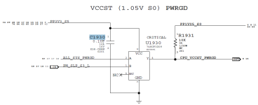
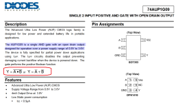
The schematics is shown in the attached picture. The output is used to produce 1.05V (PP1V05_S0). My first impression was that this is an logical AND gate. According to the datasheet: The AUP1G09 is a single AND gate with an open drain output designed for operation over a power supply range of 0.8V to 3.6V. But the actual Bollean formula is for NAND gate.

The complete datasheet is here: https://pdf1.alldatasheet.com/datasheet-pdf/view/473494/DIODES/74AUP1G09.html

Can you please clarify this?
This circuit is supplied by 3.3V. So, if both inputs (A and B) are high (3.3V), what is the output of this IC chip? From schematics it is supposed to be 1.05V after resistor 10 kOhm.

Thank you.

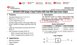
EDIT: This must be error in the data sheet because I found teh similar circuit produced by IT and there is different Boolean formula.
 

Attachments

  • C1930.png
    C1930.png
    37.2 KB · Views: 4
  • NAND.png
    NAND.png
    68.8 KB · Views: 2
  • TI AND.png
    TI AND.png
    59.4 KB · Views: 0
Last edited:

2informaticos

Administrator
Staff member
As specified, its output is open-drain.
So, you can discard output MOSFET, when inputs are both high; like deleting it from datasheet.
Guess which will be the output voltage then.

Its output generates a power good signal, not a voltage rail.
R1931 is a pull-up resistor; needed because of the open-drain output.
 

Askaleto

Member
According to the truth table given in the datasheet, if both inputs are high (3.3V), the output is in the "Z state", whatever that means.

When MOSFET works as a switch, and if Vcc is connected to the drain, and source is on ground, if the MOSFET is ON (conducting), Drain is connected to the source and the coltage is zero. When MOSFET is not ON (blocked state), the voltage on the drain is not Vcc but floating?.
Open Drain means that volatge is not equal to Vcc
 
Last edited:

piernov

Moderator
Staff member
Yes, with open-drain output, when output MOSFET of the IC is off, the output is high impedance, ie. not driven, or floating. So something else is driving it, which is the pull-up resistor R1931, pulling it to PP1V05_S0.
So in this case CPU_VCCST_PWRGD will be 1.05V if ALL_SYS_PWRGD and PM_SLP_S3_L are high (3.3V).
It is redundant since PM_SLP_S3_L needs to be high anyway to have ALL_SYS_PWRGD high, so in fact this circuit simply acts as a level shifter. Meaning that it converts the 3.3V level of ALL_SYS_PWRGD to the 1.05V level of CPU_VCCST_PWRGD.
When ALL_SYS_PWRGD is low (or PM_SLP_S3_L), then the output MOSFET of the IC is turned on, pulling the output to ground, so in that case CPU_VCCST_PWRGD will be 0V.
 

Askaleto

Member
Thank you piernov, but this is exactly what is hard for me to comprehend. If the output is floating, how come that pull up resistor ensures exactly 1.05V? All voltages around IC are 3.3 V and yet this 10 K resistor with 5% tolerance will pull up voltage to 1.05V so aacurately and precisely?
 

piernov

Moderator
Staff member
There's nothing else on the line to pull it down, so yes it'll be around 1.05V. It doesn't really matter that the voltage isn't *exactly* 1.0500…V so 5% tolerance on the resistor which will translates to a possible +/- 5% on CPU_VCCST_PWRGD doesn't matter. PP1V05_S0 itself will not be *exactly* 1.0500…V to begin with.

To be quite exact there are still some very small leakage current in the 74AUP1G09 even when the output is high impedance, it is specified in the datasheet as Ioz at around 0.2mA if Vo is pulled up to 3.6V, which translate to a resistance to ground of around 18Mohms (it's most likely not linear but let's assume that it is).

So that chip and the pull-up resistor form a sort of voltage divider between PP1V05_S0 and CPU_VCCST_PWRGD.
So the voltage on CPU_VCCST_PWRGD is 1.05V × 18Mohms / (18Mohms + 10kohms) = 1.0494V. So it has a very negligible impact.

On the CPU_VCCST_PWRGD line you also have the CPU, which also has a very high input impedance. I don't know what's the exact value, but the resulting voltage drop on CPU_VCCST_PWRGD will also be very negligible.
 
Top